

In January 2020, the International Laboratory of Quantum Optoelectronics was opened in Saint Petersburg under the Higher School of Economics (HSE). Saint Petersburg’s school of physics has always been renowned for its ideas and achievements, which were awarded with many prizes by the global scientific community, including the Nobel Prize won by outstanding scientist Jaures Alfyorov. Today, his disciple Aleksey Yevgenievich Zhukov continues to dive into the Nanoworld creating quantum-dot micro lasers for optoelectronics of the future jointly with the young employees of new laboratory under HSE. In the interview for Scientific Russia, he dwells upon quantum dots – superconductor nanocrystals with given properties that can be controlled. What are they required for? To what extent is the goal attainable? Read it in our material.
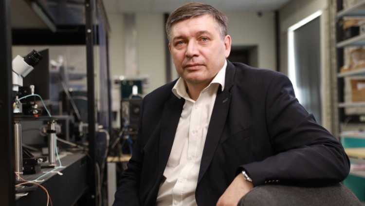
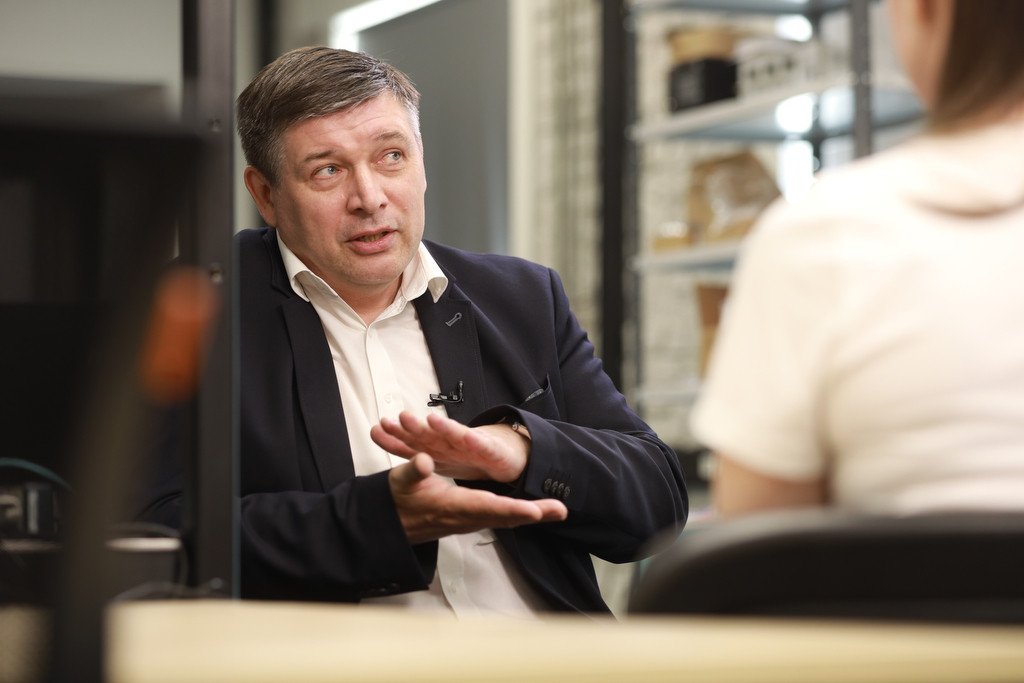
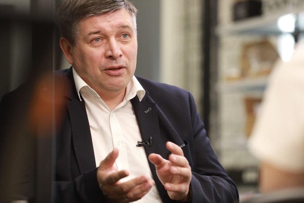
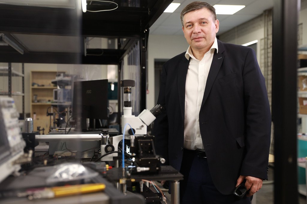
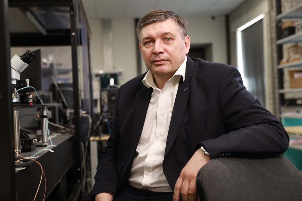
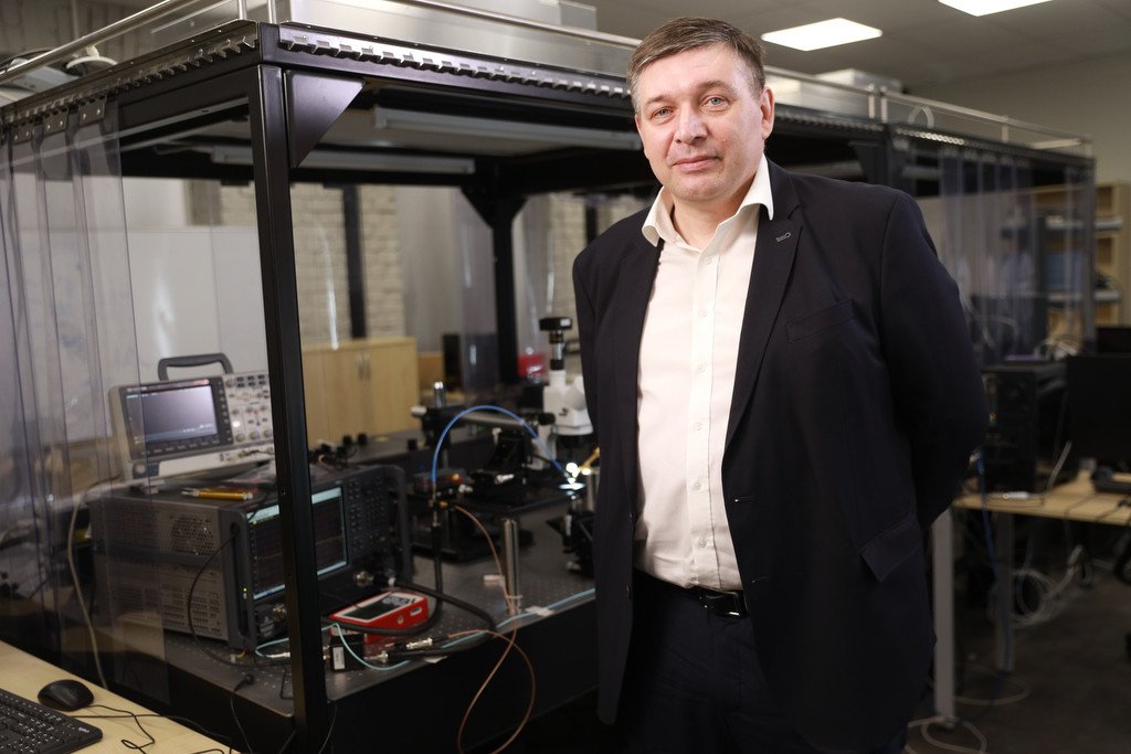
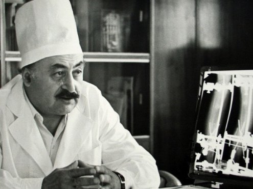
Aleksey Yevgenievich Zhukov, RAS correspondent member, academic director of the International Quantum Optoelectronics Laboratory at the Higher School of Economics (HSE) in Saint Petersburg.
Photo: Nikolay Malakhin/Scientific Russia
– What are nanostructures like? Why is such an interest in them observed today?
– Actually, the interest in them has arisen much earlier. It is that we have approached such a stage in development of science and technologies today that we cannot do without nanostructures. While this area was believed to be just an interesting line of research in physics before and developed in the form of curious experiments, now it has come to the level of real tangible products which are around us. Light-emitting diodes, lasers, transistors – all these things are actively used in everyday life today.
I have chosen optoelectronics a profession a while ago. The semiconductor laser is the most vivid example of using nanostructures in this field. 99% of lasers have the so-called quantum well as the active area where light is born. It limits the mobility of particles from three to two dimensions making them move inside the flat layer.
Small size of nanostructures gives way to new effects that are not intrinsic to a voluminous semiconductor. One of such effects is known as size quantization. Its mechanism lies in the fact that the area where electron live is reducing in size. The area becomes cramped for them, so they start rearranging forming a crystal inside the existing crystal. The example of typical manifestation as to size quantization is the control over radiation wavelength with the help of structure thickness. For instance, company Samsung has launched a line of QLED television sets. Q stands for quantum dot. Naturally, the technological principles are a bit different, but the intrinsic physical principle is the same – the wavelength depends upon the size. In polychrome displays, each pixel contains red, green and blue subpixels. These colors are combined with different intensity for obtaining millions of shades. As for the transistors containing a quantum well, for instance the ones based on indium-gallium arsenide (InGaAs), they allow for achieving higher mobility of electrons and therefore high-speed performance.
– So, these technologies have become a part of our everyday life already, haven’t they?
– Yes, years ago. The concept of using size quantization in respect to lasers based on quantum wells was formulated for the first time by Robert Dingle in mid-1970s. The idea of semiconductor quantum wells, in its turn, has become the development of the one dealing with semiconductor heterostructures formulated by Jaures Alfyorov in early 1960s.
In the quantum well, the electrons can move freely only in two dimensional directions – along the surface of the layer – while the movement in the third direction is limited by other layers. A for the quantum dot, it is a spatial domain where the carrier quantization is manifested in all three dimensions.
Here, I will take the liberty of praising myself and my colleague from the Ioffe Institute of Physics and Technology. The first laser on quantum dots was made here, in Saint Petersburg in 1994. I was lucky to take part in this work. We were the first to grow lasers with quantum dots. It was a real breakthrough! Everybody realized that Russian science is capable of creating advanced technologies.
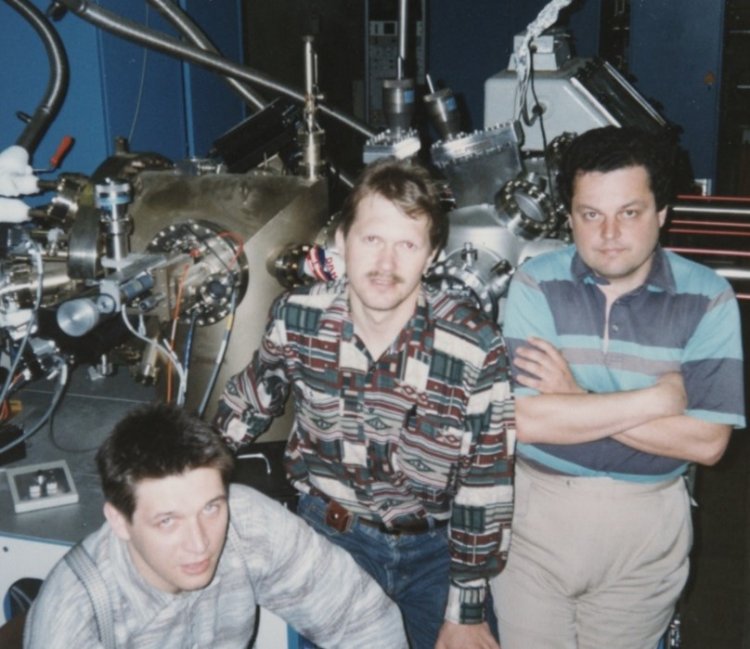
The group for studying molecular-beam epitaxy of the Ioffe Institute of Physics and Technology: V.M. Ustinov (right, at present RAS correspondent member, director at the Research and Technology Center for Microelectronics of RAS), A. Y. Yegorov (center, at present RAS correspondent member, technical director at Connector-Optix LLC) and A. Y. Zhukov (left) in front of a newly launched molecular-beam epitaxy facility Riber 32P. 1996
– Where do quantum optoelectronic instruments find application today?
– The most knowledge intensive sphere is the one of optical communication with fast information transfer. It is clear that its share is increasing every day. It means that transmitting information across the wires become impossible due to limited product of distance range multiplied by data transmission rate. Simply put, the data transfer to long distance is slower. Optic fiber can boast of a higher product of distance range multiplied by transfer rate if compared to wires.
Today, we use fiber-optical lines in house, offices and at garden plots. The next stage is implementing optical communication in supercomputers, of global Data centers. Subsequently, the range of communication in the fields where optics is used is gradually reducing. In the time following, each computer is expected to have its own optical system or optoelectronic board. The same is true for smartphones.
The goal that we look forward to is optical circuit inside the chip. In fact, our teachers laid the foundation for optical communication 40 year ago creating lasers. Why did Jaures Alfyorov become a Nobel Prize winner? It is because he invented semiconductor heterotructures and created the first instruments on their basis. Unfortunately, the Nobel Prize was awarded to him for that many years later.
– Yes, it is typical of the Nobel Prize, isn’t it?
– You are right. I remember well the day when Alfyorov became a Nobel Prize winner and the outburst of emotions experienced by all employees of the Ioffe Institute. Buy the way, he invited me to the awarding ceremony in Stockholm. It was a real euphoria: Russian scientist won the Nobel Prize.
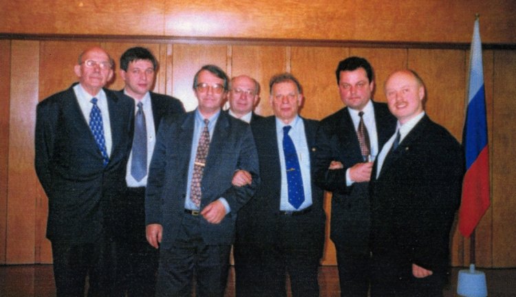
Banquet at the Russian Embassy in Sweden in honor of the Nobel Prize winner. From left to right: B. P. Zakharchenya, A. Y. Zhukov, P. S. Kopiev, V. I. Kuchinsky, J. I. Alfyorov, V. M. Ustinov, N. N. Ledentsov. Stockholm, 2000
– What has been achieved over the 50 years?
– The most tremendous progress. What was the advantage of Alfyorov’s heterostructures? With the help of them, we managed to build a laser working at room temperature. Besides, the emission power was low. When I started dealing with this research area, powerful lasers with power of 1W appeared at the Ioffe Institute. 10 year later their power rose 10-fold and even more.
The same is true for data transfer rate and distance range. While 1Gb/s data transfer has seemed an ultimate dream before, the one of 20-30Gb/s is no big deal today.
– When speaking about nanostructures, they often mention molecular-beam epitaxy method. What about its specifics?
– Just imagine a structure in the form of layered semiconductor cake. The point is that required layers are being grown on a crystal substrate, some of them being quantum-sized ones. How does the method work? A substrate is placed into a vacuum chamber with the air and all unnecessary substances having been pumped out of it, and the required elements are then grown on this substrate. The starting substance is kept in the crucible – a sort of pot made of heat-resistant glass. Gallium and arsenic represent the most common type of starting substance. The elements warm up and fly to the crystal substrate to combine there.
– Why is it important to grow the elements in vacuum?
– First, high grade of vacuum ensure purity. Second, molecules fly like bullets in vacuum without changing the trajectory. That is why it is easy to block the flow of atoms in vacuum with the help of simple mechanical shutter. It allows for creating various heterotructures. You open the aluminum shutter and gallium-arsenic becomes aluminum-gallium-arsenic. Open the one for indium – and you will get indium-gallium-arsenic.
Actually, we can change the chemical composition on the level of monolayer, i.e., atomic later. At present, it is one of the most advanced technologies for creating semiconductor heterostructures for optoelectronics.
– Do end-use properties depend upon the starting substance?
– Upon both the substance and dimensions. In pre-quantum period, the selection of required chemical composition remained the only method to change, say, the wavelength. Yet, certain restrictions were even here. First of all, it was to be consistent with crystal lattice in parameters and tolerate certain temperatures.
As it has turned out, the quantum well is thin and can be grown on substrate with different crystal parameters. Put it simply, the quantum well can adjust within certain limits. Besides, we can adjust the wavelength changing the thickness.
– You have talked a lot about quantum dots, wells and future of optoelectronics. Some specialists are active in creating a quantum computer today. Are optoelectronic principles used in this field or these areas do not overlap?
– Naturally, they are used. These spheres really overlap. However, it is not yet clear which method is the most efficient one for creating a quantum computer, and what principles the data transfer inside its elements should be based on. Anyway, the optical communication is always better than wire transfer from the viewpoint of action speed.
Besides, quantum cryptography is very closely adjacent to the sphere of quantum computing. Here, the principles of quantum optoelectronics are used without question, in particular ingle photon sources. The matter in question is about communication that cannot be deceived, as the properties of received signal change if someone wants to steal it, while the receiver learn about it at once.
The single photon sources are based quantum dots each of which can emit single photons, as one quantum dot generate a single photon in unit time.
– Let us talk about your laboratory which has been founded very recently. When and how did the idea of its foundation arise? What have you come to today?
– The idea has been germinating for a long time. I am grateful to HSE management for the decision to deal with physics. This very decision resulted in our laboratory. Formally, the laboratory opened its doors in January 2020. The Higher School of Economics allocated a large amount of money for purchasing the equipment. It is what we were dealing with for the whole COVID year.
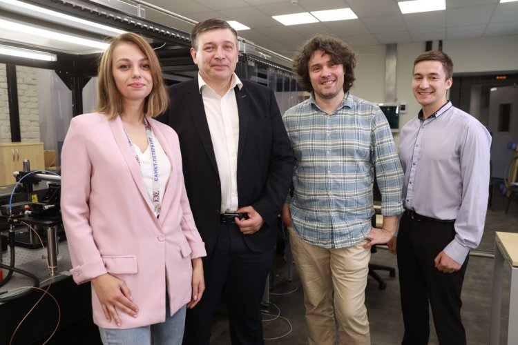
Employees of international quantum optoelectronic laboratory of HSE. From left to right: manager Yelizaveta Kotko, academic director Aleksey Yevgenievich Zhurov, leading research fellow Aleksey Nadtochiy, research fellow Eduard Moiseyev.
Certainly, we came across certain difficulties. All the communication with suppliers had to be conducted remotely. Fortunately, the equipment has been purchased and installed by today.
We at the international laboratory of quantum optoelectronics place emphasis on the research related to micro lasers. Straining after the cross-breeding of optical communication and microchip, we have to reduce the dimensions of laser.
Special optic measurement equipment that allows studying tiny objects helps u in the work to this end. Along with this area, we take interest in rapidly changing processes: fast measurement of optic signals and their modulation. Both of them provide information as to how fast we can exchange data with the help of such a laser source, how fast we can transfer information, what intrinsic constraints are present.
Besides, our studies are aimed at measuring temperature as well. It is important to make an instrument capable of working at room temperature or higher one which is even better.
– What is the application aspect of it?
– The laboratory employs people who have come of academic institutes. That is why we our mission in investigative studies above all. Naturally, each of the areas has a clear application prospect. However, when it comes to application, we hope to have people nearby who will pick up our technologies and start implementing them directly into production.
Unfortunately, our scientists managed to develop technologies of quantum dot lasers only in the West. Now, the situation has changed for the better a bit. There is hope that this line of research will tart being developed in Russia in the application aspect as well.
Today, many scholar groups are trying to create an optic laser source capable of transmitting information among silicon integrated circuits or even inside an integrated circuit. However, a number of requirements have to be complied with: such a source should be capable of working at higher temperatures; it ought to be small and compact, as well as integrated with silicon. It stands to mention that silicon is a very specific material which does not produce light, yet is the basic element in electronics. That is why many fundamental problems still require solutions.
– Who could be the end user of such technologies?
– The group of end users must include the companies dealing with development and production of silicon electronics and silicon integrated circuits, or the ones working in the field of optic communications. Today the spheres of optic communications and microelectronics develop separately from each other. Some in-between technology must bring them together. This is what we see our mission in – bringing these two areas together. Now, we try to establish such contacts.
– What equipment do you use?
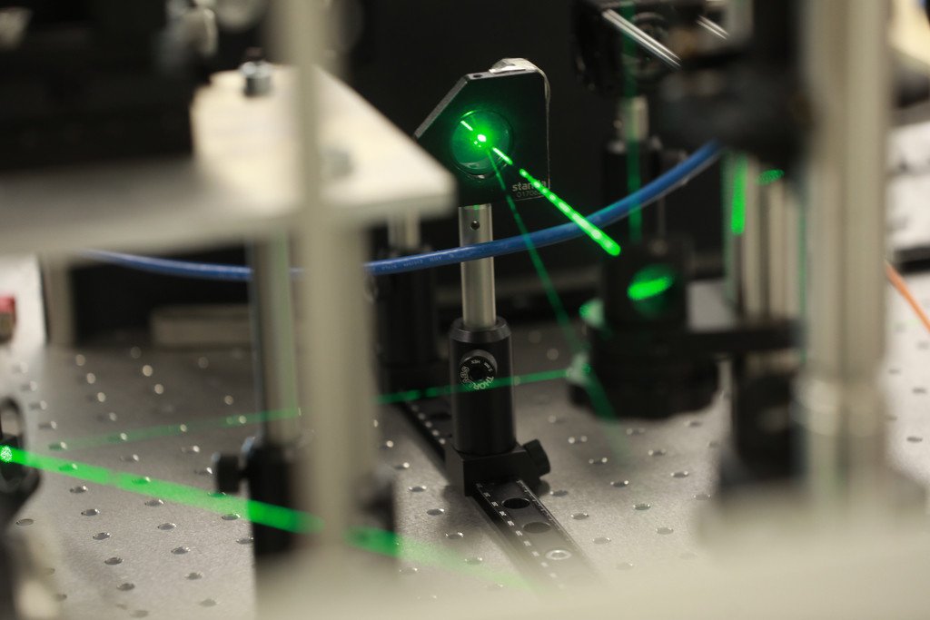
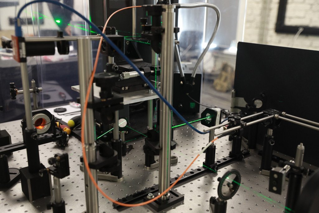
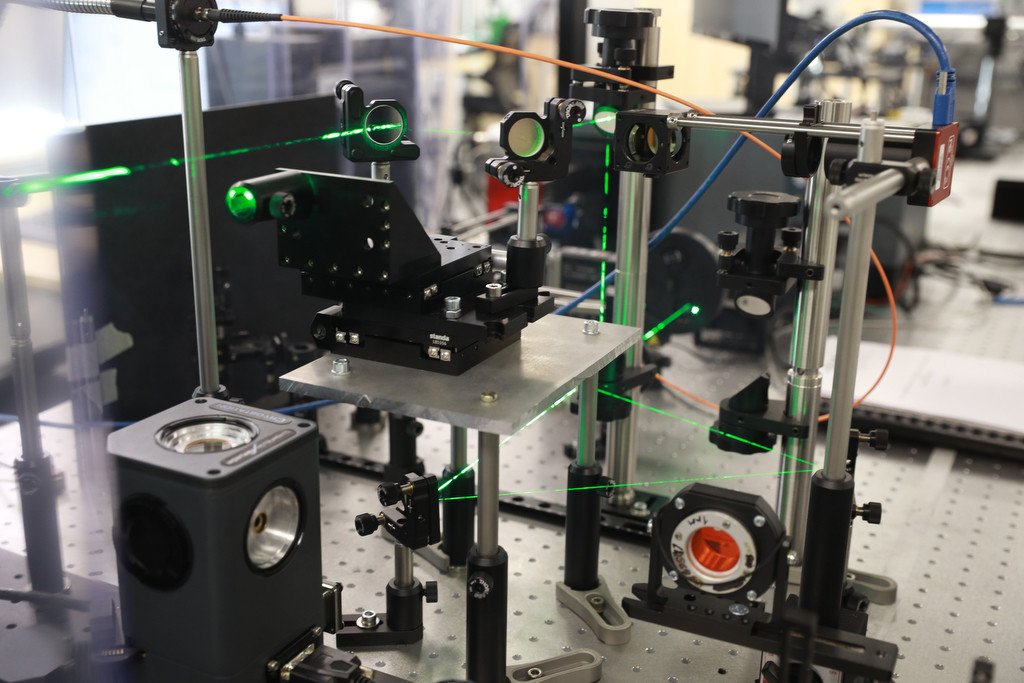
– The laboratory I equipped with unique research facility Comprehensive Optoelectronic Stand. As for quick measurements, we use the so-called time-resolved luminescence. Our employees are now testing, adjusting and calibrating this instrument.

Part of equipment of Comprehensive Optoelectronic Stand facility
Along with that, the method of high-frequency modulation is used: we change the emission intensity with the help of fast signal and watch the response. Naturally, we cannot do without thermostatic cooler (cryostat) in our research. Modern cryostats are different from the gigantic reservoirs where one should pour liquid nitrogen and helium. Now, they are more compact and user-friendly.
Vibration-resistant optic table is the basis of the facility. It allows for avoiding unnecessary vibration and provides for the accuracy of measurement even for very small objects.
– Are there any interesting results that you can share?
– Sure. Recently, we have published a serious survey devoted to quantum dot micro lasers in top-rated journal Light: Science & Applications. In general, we have managed to make a micro laser working at 110 degrees Centigrade. We have demonstrated optical data transfer at the rate of 10 Gbit/s. It is not a record for lasers in general, but a very good performance for micro lasers. All these achievements bolter our confidence in having chosen the right way.
– How did you take interest in this topic?
– Let me begin in a roundabout way. Being a boy, I went to St. Petersburg-based physics and mathematics school which is now known as Presidential Physics and Mathematics Lyceum No 239. After finishing school, I started thinking about further education. It so happened that two of my mates took interest in the optoelectronic department founded by Jaures Alfyorov. As we were on friendly terms, I decided to enroll with them, though I had no idea as to optoelectronics and Alfyorov at that time. However, I submerged into the atmosphere learning with a man really dealing with research being my teacher. It was clear to us what we had to aim for.
Students were drafted into the army at that time, so I came back to the institute only after two years of army service. At that time there was no postgraduate job assignment, so I had to strike out in my own after graduation and decided to develop the topic of my diploma paper. A new research group was organized at the Institute of Physic and Technology, and I joined it. At that time, a new molecular-beam epitaxy facility was built. With the help of modern instruments, advanced for that time, our group crated and demonstrated the world’s first quantum dot laser. This achievement allowed us to win a reputation among scientific community. We started actively contacting with various research institutions and schools including the colleagues from the Technical University of Berlin. By the way, I still can boast of close ties with them. Very soon, I defended the candidate’s thesis and later the doctoral one.
However, I still take interest in optoelectronic and semiconductors, especially micro lasers on quantum dots.
– Is there any interest on the part of foreign colleagues? How do you keep in touch with them today?
– At present, we communicate with them in remote format, yet the interest on their part still exists. In Germany, for instance, my friends have founded a company for producing semiconductor lasers. We not only consume their products, but hare the ideas and experience with them.
Besides, we have connections with a group of scientists at the University College London. They deal with silicon epitaxy and we are active in cooperating with them. A laboratory named after Jaures Alfyorov was founded at the Beijing University of Posts and Telecommunications, where I worked as visiting professor before the pandemic. We have visited this educational establishment with lectures often enough and conducted joined research with Chinese colleagues. This cooperation continues today as well.
– At the beginning, you have outlined a certain way from optoelectronic communication to microchips. When will this result be achieved, based on contemporary trends?
– The patent for using quantum effects in lasers was issued in 1979, if I am not mistaken. The operational instruments appeared in late 1980s – early 1990s, i.e., 11 years later. As scholars have been dealing with this research area for 5 years already, we should expect the first results in some 6 years. In general, experimental prototypes of optical communication among chips have been demonstrated already, so it won’t be long till implementation starts.
Interview taken with the support of the Science and Higher Education Ministry and Russian Academy of Sciences.


