

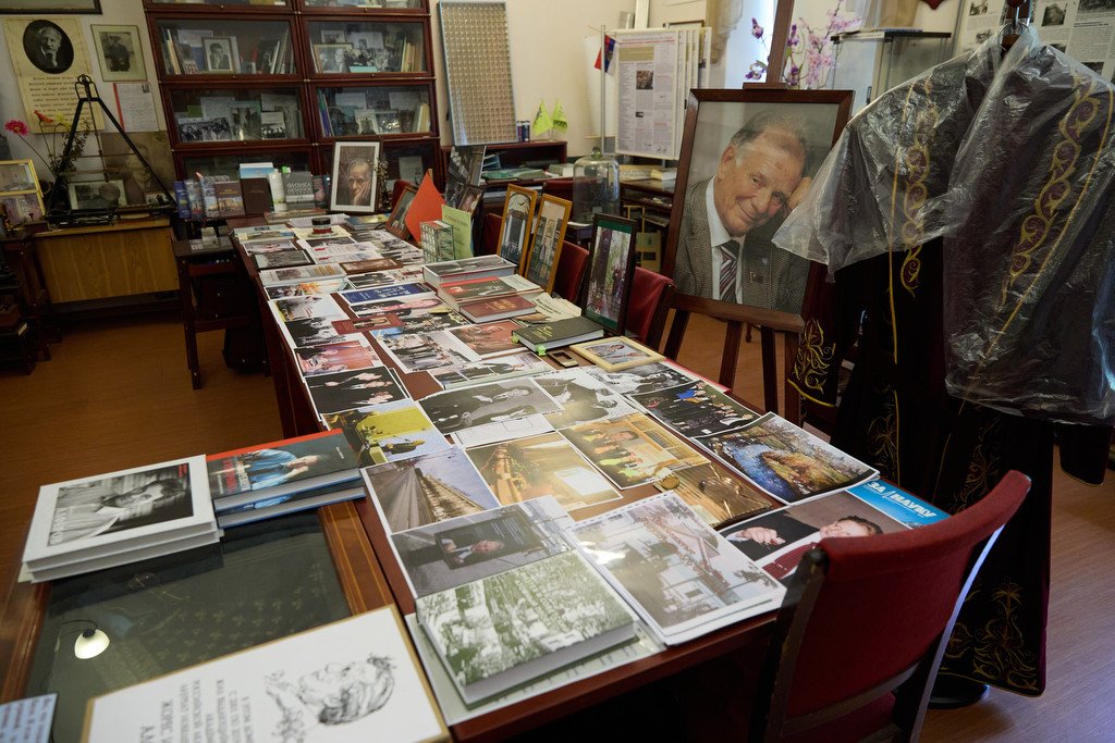
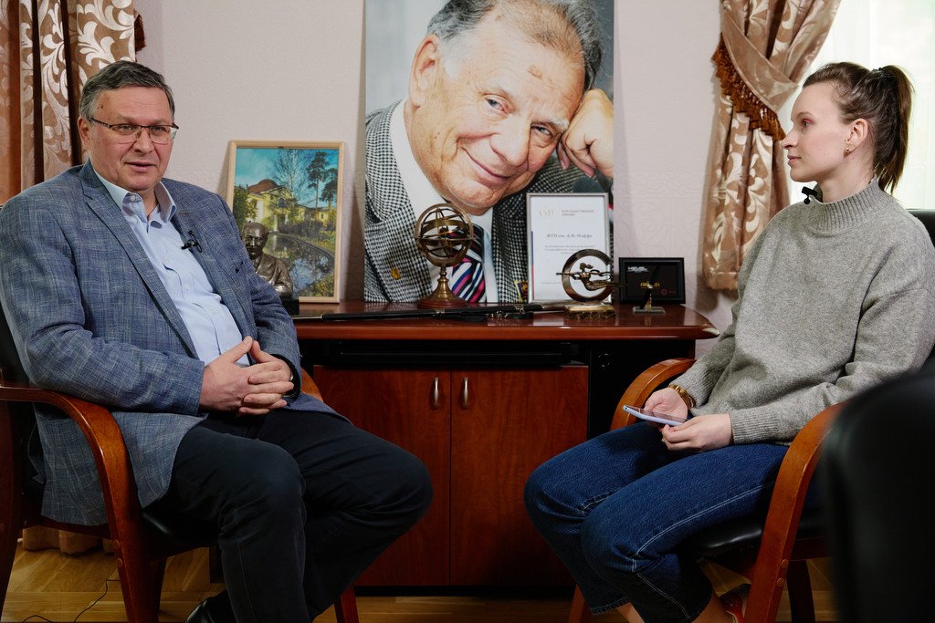
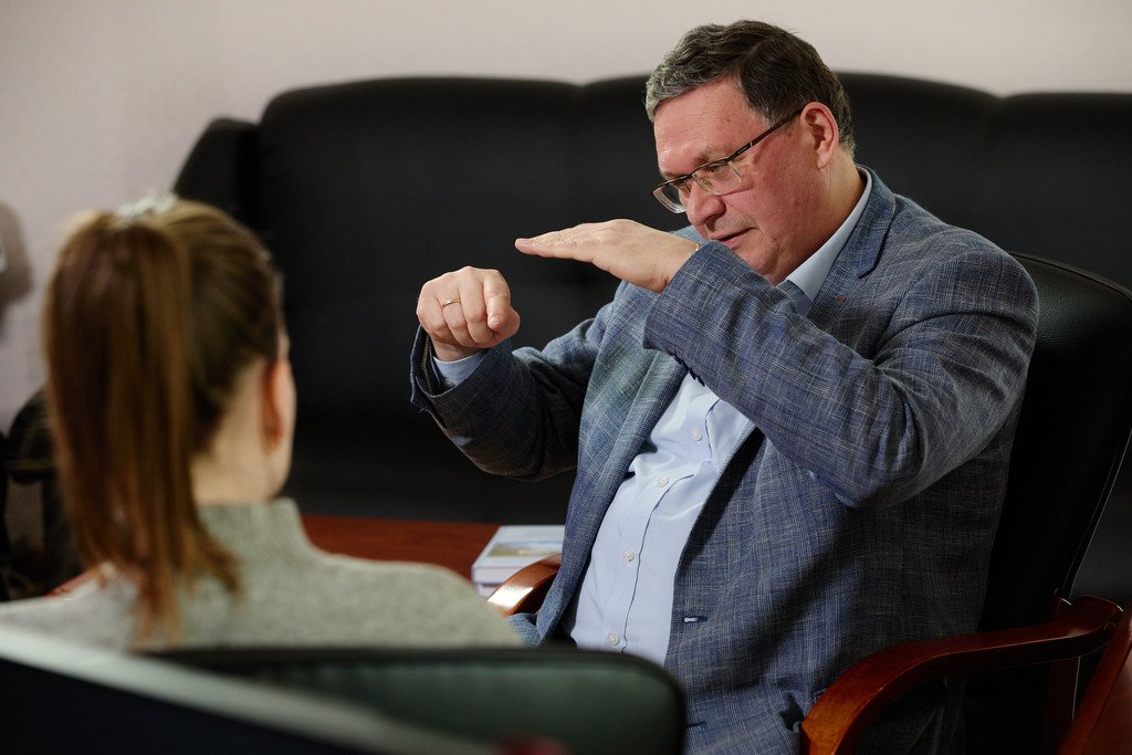
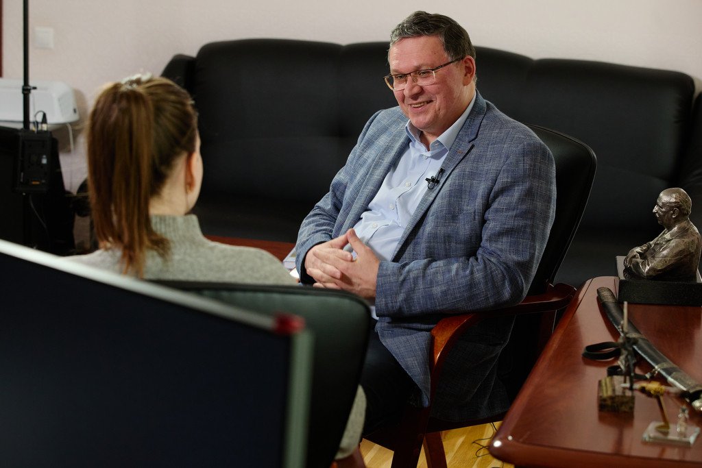
The Ioffe Institute is generally considered to be the cradle of Russian theoretical and experimental physics. It was there where outstanding scientists, including Nobel laureates Nikolay Semenov, Lev Landau, Petr Kapitsa, and Zhores Alferov started their research career. Today the Ioffe Institute scientists continue their research at the forefront of science, without forgetting the experience of their predecessors, who made the national school of physics famous all over the world. The Ioffe Institute Director, Sergey Ivanov, said there are small hearths of Russian physics everywhere around the globe, and very often they are originally from Ioffe Institute. We have talked about these things and more in the interview with Sergey Viktorovich Ivanov.
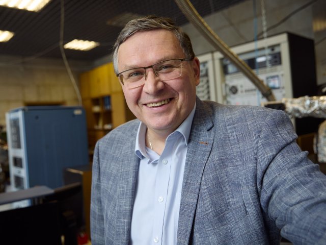
Sergey Viktorovich Ivanov – Director of Ioffe Institute, Doctor of Sci., professor
– Zhores Alferov's works were awarded the Nobel Prize. It was he who determined further development of the semiconductor heterostructures topic. Do scientific trends in modern physics depend on outstanding personalities or world awards?
– They do not depend on awards, of course, but they do depend on personalities. The progress may be slow or it may be fast. If we talk about research on heterostructures, this topic was studied independently in several laboratories around the world, including our own, the Ioffe Physical-Technical Institute (PTI). In fact, this research was being conducted simultaneously, and the employees of competing laboratories knew about each other. This fact suggests that the discovery would have happened anyway. Meanwhile, the “competition” of scientists and the exchange of experience (Zhores Ivanovich traveled to the United States and met foreign colleagues from the Bell Lab.) somehow stimulated this progress. In the end, the Soviet scientists won.
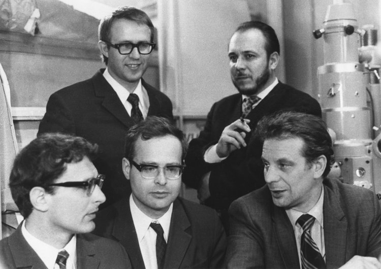
The great Alferov’s team at the PTI in 1970 that created the world's first continuous wave laser diode based on the double AlGaAs heterostructure operating at room temperature. From left to right: D. - Z. Garbuzov, V. - M. Andreev, V. - I. Korolkov, D. - N. Tretyakov, Zh. - I. Alferov
One should say that our scientists understood well from the very beginning in which direction to move. Nevertheless, this discovery, as always, was born in agony. At that time, the Physical-Technical Institute was actively involved in R&D of bulk semiconductors, powerful germanium and silicon diodes, thyristors, which electronic and power industries needed. They also studied laser structures based on bulk III-V semiconductors. Our scientists tried to produce intense spontaneous (LED) and laser radiation from binary bulk semiconductors doped with impurities of different conductivity.
Zhores Alferov and his colleagues suggested that a semiconductor heterostructures, employing all the advantages of intentionally varied energy spectrum in a semiconductor crystal, would be able to diminish the influence of undesirable defects which inevitably arise when we try to integrate semiconductors of different chemical composition in a single crystal. However, this point of view, of course, met with resistance and misunderstanding. Therefore the discovery of the technological possibility to realize nearly ideal (defect-free) semiconductor heterostructures by Alferov's group made a real revolution. So when it turned out that the semiconductor laser parameters could be improved by at least tenfold, everyone realized that this was the only way to work with. And the usual homo-optoelectronics of that time was put on the back burner.
– What was achieved in these 50 years?
– Actually, it will be 50 years in 2022 since the first semiconductor heterolaser operating in cw mode at room temperature was created. Over the years, the spectral range of semiconductor lasers has expanded significantly.
Traditionally, lasers were based on a single AlGaInAs group of III-V materials. Therefore, they had a limited number of specific applications. They were mainly used in the field of fiber-optic communication lines. Later, the concept of heterostructures was applied to the III-V (third and fifth groups of the Periodic Table of chemical elements) semiconductors of other chemical compositions as well as other groups of the Periodic Table (II-VI by analogy). And as we know, changes in chemical composition, atom size, strength of chemical bond and its ionicity lead to a variation of the energy spectrum of semiconductors, and therefore, the emission wavelength changes. It became possible to change its value significantly: from 500 nanometers to several dozens of microns.
Besides, new wide-gap materials were discovered, namely group-III nitrides, which are capable of emitting in the ultraviolet region (up to 230-300 nm). It was known that all III-V materials possess semiconducting properties, but the latter were not technologically accessible. But later, such technologies were invented and upgraded. Today, the entire range of semiconductors from indium antimonide to aluminum nitride is used to create semiconductor photonics devices.
On the other hand, the range of such photonic devices expanded considerably. Zhores Ivanovich started with conventional diode lasers, followed by heterostructured lasers. Later, physicists began to work with a next level of quality and quantum-size heterostructures appeared. They are also called low-dimensional heterostructures. The word “dimension” is important because it is already comparable to the De Broglie wavelength of an electron in a semiconductor. In other words, an electron, being in a small limited volume, simultaneously feels both walls of the potential well, so it becomes a quantum particle, and its energy spectrum is quantized, i.e. separated into discrete energy levels. The idea is simple: the classic aluminum-gallium arsenide is used as a barrier material. The quantum well layer is made of gallium arsenide. The alternation of layers creates an energy spectrum of the structure in the shape of a rectangular well. It can be wide or narrow. Modern technologies, such as molecular beam epitaxy, allow the thickness of grown layers, comparable to the quantum size, to be controlled with an accuracy of a single monolayer. Therefore, it is possible, to achieve a variation of the emission wavelength by changing the energy of quantum levels owing to variation of the quantum well layer width, without changing the layers chemical composition.
Thus, quantum mechanics had found its application in semiconductor structures. This has given it a new practical quality. With the help of quantum-size effects it is possible to obtain fundamentally different properties of materials, fundamentally different parameters of devices in terms of both electrical and optical properties. This allowed one to make a transition to quantum dots, i.e., objects in which charge particle motion is limited on all three sides, and, therefore, the spectrum of electron (hole) states represents a delta function; in other words, there is one pair of energy levels in the active region with a strictly defined radiation wavelength.
If we talk about the development of novel device design, the so-called quantum-cascade lasers have been added to diode ones. They imply that only one type of charge carriers, say, an electron, is involved in the emission processes. Such a quantum-size heterostructure contains multiple ultrathin layers and represents a series of cascades in which the electron first rises smoothly up the quantum staircase to a high quantum level, then drops in the quantum well to a low level, emitting a quantum of light. Then it enters the next injector again, where its energy rises smoothly in the applied electric field, and then it loses the energy again. A kind of stepped waterfall. The performance of quantum-cascade lasers was theoretically described in 1971 in the Soviet Union by R. F. Kazarinov and R. A. Suris, while they were first implemented in 1994 by the Bell Laboratories using molecular beam epitaxy, which was invented there as well.
The lowest-threshold lasers with quantum wells were developed at the PTI at the end of the 1980s, and in the 1990s, it was Ioffe Institute where the world's first quantum dots lasers appeared, both III-V (in 1994) and II-VI (in 1999). So, a certain parity between PTI and Bell Labs is still preserved. Many things have changed, but the basic principles were laid down 50 years ago.
– How did scientists learn to interact with the quantum world? The quantum was always considered to be something elusive, inaccessible.
– It took quite a long time. It took about 30 years since the first semiconductor lasers and LEDs appeared, until the first single-photon sources emerged (and this happened approximately at the end of 20th century). When the physics of these single-photon sources became clear, specialists immediately began to create physical objects. One of the basic and most promising objects turned out to be a semiconductor quantum dot.
A quantum dot has a discrete spectrum. This means that radiation can occur only from a certain quantum level in this dot. It is strictly deterministic in terms of energy, i.e. wavelength of radiation. And since one electron only can occupy the level in a quantum dot at a time, a single act of radiation gives birth to a single photon.
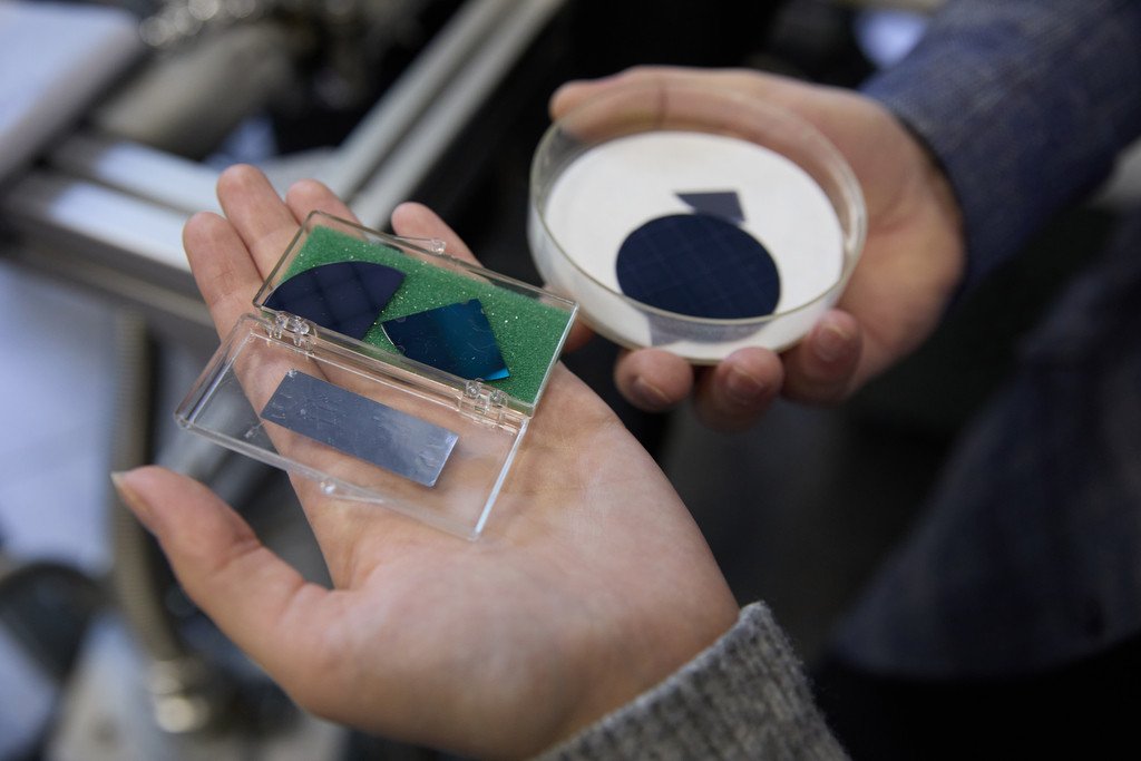
Using this principle, it became possible to develop not only epitaxial technologies that produce semiconductor nanoheterostructures with self-forming quantum dots, but also to make significant advances in planar processing technologies, e.g. reactive ion etching technologies. The point is that the quantum dots are arranged in a plane in the fabricated heterostructures. There can be many such dots – about a billion per square centimeter, although this density is considered as low. But it is possible to isolate, say, a small circle in a plane, or to create the so-called mesa-structure, being a nanocolumn with a diameter of 200 nanometers, which has in its base no more than ten quantum dots.
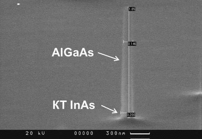
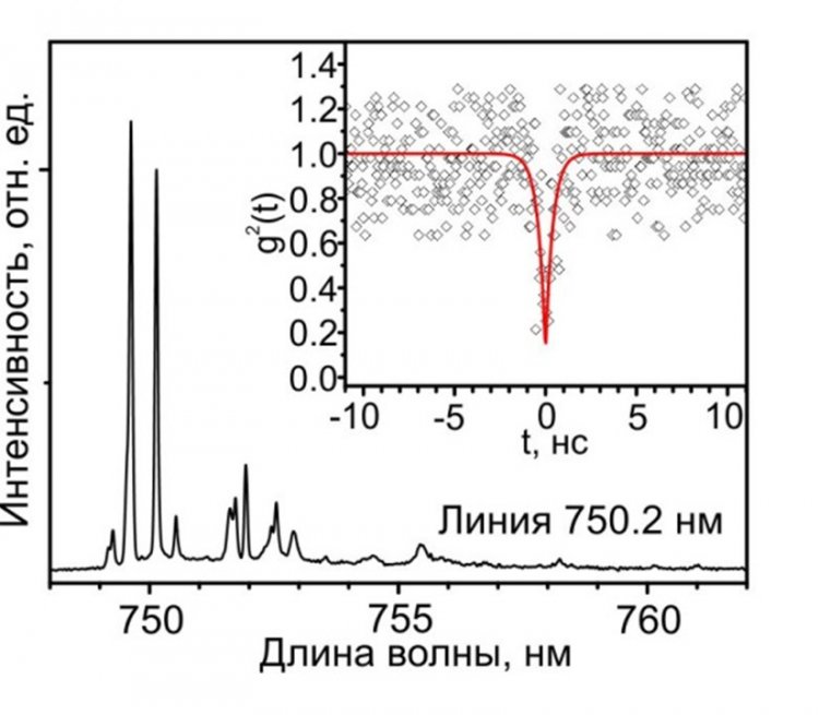
Microphotograph of a single photon source nanocolumn (up). Typical microphotoluminescence spectrum of a nanocolumn with narrow lines from single quantum dots and a second-order autocorrelation function for single-photon emission of InAs/AlGaAs QD at 750.2 nm down).
– Why does it happen?
– This is how they are distributed in the plane, and we choose only a few quantum dots in a limited circle of the plane. A microscope with good resolution makes it possible to excite and collect radiation from a particular nanocolumn. Usually, a whole matrix of such columns is created. The task is to find a corresponding object, in which the intense emission comes from a single dot with the desired wavelength. This is visible in the emission spectrum of such nanocolumns, which is separated into a series of narrow lines depending on the energy. Among them, there is often a line of high intensity with the necessary wavelength. It is important to select spatially a particular nanocolumn optical system with an accuracy of tens of nanometers and highlight spectrally radiation in a particular quantum dot.
This became possible after both optical techniques and planar technologies were developed simultaneously with the precise epitaxial technology, and single photon detectors that can register the passage of a single photon became available.
– How do they work?
– It's pretty simple. Two photodetectors are installed with a semitransparent mirror in front of them, which allows the incident light flow to separate. If two photons fly simultaneously, both photodetectors will show a signal at zero time. If it is a single photon, only one photodetector will register the radiation. Therefore, the so-called optical correlation function is measured, in which registration of photodetectors is separated in time, allowing them to register simultaneously signals from different photons coming from the object. And a correlation dip is formed when the moment of photons registration time gets closer – this is a correlation function. It serves as an evidence that the device registers single photon emitted by the dot.
If you send such single, and even indistinguishable, i.e., identical in all parameters, photons in a waveguide matrix with interference effects, designed in a certain way, it is possible to create a simulator of optical quantum calculations. In Russia, such nanostructures are fabricated only at our Ioffe Institute, in the laboratory of Alexey Akimovich Toropov, and are applied in the laboratory of Sergey Pavlovich Kulik, at the Physics Department of Moscow State University. In this case, single photons play the role of qubits in quantum computing. But this is not their only use.
– Today the scientific community is increasingly talking about some kind of extreme conditions. What are we talking about and what perspectives can it offer?
– In the context of our conversation, we can mention the extreme size and extreme accuracy of creating the quantum objects. And this is a really serious problem that rests on the correct organization of the technological process. For example, when such multilayer nanostructures are grown for many hours, a slight fluctuation of temperature in the laboratory, even by 1 degree, can lead to a change in the growth rate of the corresponding material or to an uncontrolled change in its thickness, and therefore to optical imperfections in the structure.
If we talk about temperature, all studies starts at low temperatures, often at liquid helium temperatures, when we obtain the maximum quantum efficiency. But the task of specialists developing any scientific and technological ideas is to bring the devices as close as possible to normal operating conditions, i.e., room temperature and atmospheric pressure.
– In 2018, the Ioffe Physical-Technical Institute celebrated its centennial anniversary. How did the institute enter its new century? What has been achieved over the years?
– The history of the Institute is very rich. And a lot of things were laid down by our first director, Abram Fedorovich Ioffe. It was he who started both semiconductor research and studies of crystalline properties of solids with the usage of X-rays. At the same time, in 1931, thermoelectricity began to develop, and the first solar photovoltaic converters appeared, which were proposed by Abram Fedorovich for the state program of “solar roofs”.
Then the studies of the atomic nucleus began, which were also initiated by A. F. Ioffe. All the key figures of the Soviet atomic project – I. V. Kurchatov, A. P. Alexandrov, N. N. Semenov, Y. B. Khariton, Y. B. Zeldovich, A. I. Alikhanov, L. A. Artsimovich, G. N. Flerov – originated from the Physical-Technical Institute. Owing to this, a strong scientific school of atomic physics began to develop in our country. Finally, the direction of semiconductor heterostructures arose and began to develop actively.
Each of these fields presented new challenges to scientists. For example, atomic physics has moved to a significant extent into the research field of the next generation, the nuclear fusion. The Ioffe Institute is very active in the field in terms of developing technologies for heating, generation, and confinement of thermonuclear plasma. So our tokamaks are known throughout the thermonuclear world.
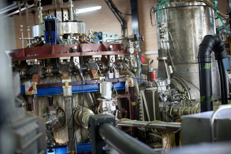
The Globus-M2 Tokamak at the Ioffe Institute is now in the top three spherical tokamaks in the world, diameter 1.5 m
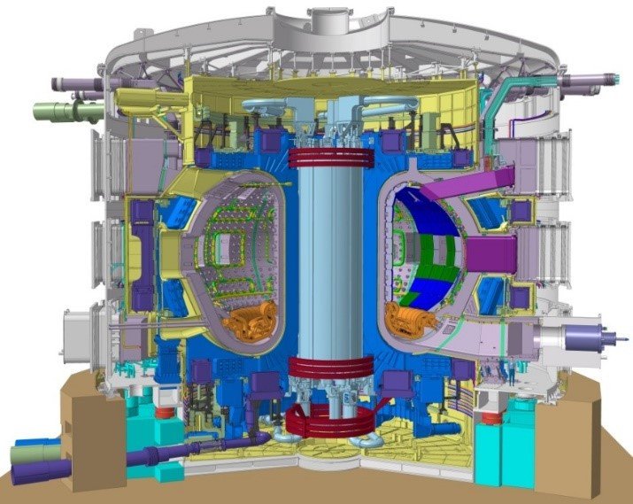
ITER reactor, Caradache, France, height 40 m
Our scientists have seriously advanced in the field of fusion plasma diagnostics using various optical methods. In particular, researchers from Ioffe Institute are participating in the International Project on the creation of the thermonuclear experimental reactor - ITER. We will manufacture and supply three types of the most critical diagnostics for this fusion reactor. In other words, the research that was initiated by A. F. Ioffe and I. V. Kurchatov reached a new qualitative level already under the leadership of B. P. Konstantinov and V. E. Golant.
Astrophysical research is also actively performed. Many recording detectors installed on orbital satellites are made at the Ioffe Institute. Our scientists participate in the international consortia for building large ground-based telescopes to record gamma-ray bursts. We also conduct research in the field of antiparticles, dark matter, and space objects with extreme energy, whose radiation can be registered in various spectral ranges.
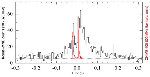
The Ioffe Institute’s detectors on the orbiting satellite Cone-WIND recorded a flare from the magnetar SGR 1935+2154, with an unusually hard spectrum, accompanied by a powerful radio burst, measured by CHIME and STARE2 radio telescopes. That allowed the first connection between galactic magnetars and fast radio bursts to be established
The semiconductor field as a whole, under Zhores Ivanovich, led to the creation of a department and, later, of the Center for Nanostructure Physics. Now the Center has about ten laboratories. Specialists ellabotrate high-power semiconductor lasers, single-mode vertical-cavity surface emitting lasers for fiber-optic telecommunications, quantum sensors, and frequency standards.
To date, the sophisticated and precision semiconductor optical devices are employed in numerous fields. There are devices based on infrared optics that can be used for a wide range of medical applications, for recording characteristic diseases identified by the chemical composition of the air we exhale. In addition, such devices are used in diagnosing industrial pollutions – the concentration of carbon dioxide in industrial plants or methane in mines, for example.
The Ioffe Institute also holds a leading position in the field of ultraviolet photonics. The Institute's experts and technologists develop technologies of sun-blind semiconductor photodetectors in the AlGaN system and environmentally friendly emitters with wavelengths of 260-270 nm, which have a destructive effect on bonds in the protein molecules of viruses and bacteria, i.e., possessing a disinfecting effect. This is very relevant at present.
We are actively working in the field of materials science. This field was once born in the Institute thanks to Nikolai Nikolayevich Semenov, who founded the Department of Chemical Physics. Later it was transformed into the entire institute, which moved to Moscow in 1934. Just recently we celebrated the 125th anniversary of Nikolai Nikolayevich Semenov's birth. The continuation of his work at the Ioffe Institute is modern research in the field of chemical physics, metaloxide and carbon composite materials used in renewable energy, including hydrogen energy, and electrode elements for various supercapacitors and high-power accumulators.
We should not forget about research in biology and medicine with the use of optical spectroscopic methods, which the Ioffe Institute possesses. And, of course, a significant part of basic research that is devoted to spintronics. Let me remind you that electrons carry not only charge, but also spin – the electron's own magnetic moment. It can be considered as a miniature magnet, which creates a local magnetic field around itself. This means that the orientation of electron spin can be changed by an external magnetic field, circularly polarized radiation, or an spin-polarized electric current. These studies were initiated at the Ioffe Physical-Technical Institute back in the 1970s – theoretical, and then experimental. Technological developments, including semiconductor, magnetic and ferromagnetic materials, and knowledge of the spin dynamics behavior allow the development of prototypes of spin transistors and memory elements. It is expected that they will significantly expand the capabilities of modern electronics in the near future.
Finally, one should mention another no less important area of activity: solar energy. These were the semiconductor heterostructures discovered by Zhores Ivanovich Alferov that were also used to create cascade solar cells. In 1987, the Soviet orbital station “Mir” was launched with solar cells developed at the PTI and produced at the scientific-industrial enterprise “Kvant”, which remains one of the main companies of Roskosmos State Corporation for production of semiconductor solar cells. The leader of this field at the Ioffe Institute Vyacheslav Mikhailovich Andreev. His laboratory employs young technologists and experts, who are able to implement such technologies on an industrial level.
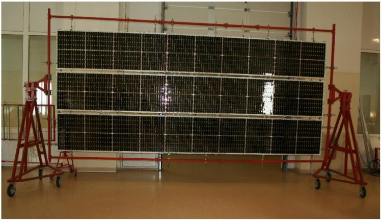
Space solar panel (~ 10 m2) based on cascade photoconverters with a 29% efficiency, manufactured at PJSC “Saturn” using the technology developed at the Ioffe Institute.
Each of these areas is supported by the unique theoretical schools of the Ioffe Institute in the field of solid-state physics, plasma physics, and astrophysics. A generation of young scientists, who become doctors at the age of 30 and corresponding members of the Russian Academy of Sciences at the age of 34, has grown up. It is wonderful that their number is growing up. Young, talented guys come to the laboratories and sectors of Ioffe Institutes and immediately get involved in the serious work and start publishing independent scientific results in the highly ranked international journals.
We also do not forget about the international cooperation with our colleagues from foreign laboratories around the world.
But right now, we are primarily focused on enhancing applied activities and bringing our developments to industry. Certainly, to a significant extent, as Zhores Ivanovich used to say, this is held back by the fact that our industry is not yet able to implement everything that is being created here in the Institute, and does not possesses the necessary equipment. But things are moving forward: domestic manufacturers of modern scientific and technological equipment are developing more and more. And we already have very successful examples of such cooperation in working with domestic technological equipment.
It is important that the developments I was talking about do not stay here at the Institute, but go into industry and are used by companies that work in the science-intensive sector. This is why the R&D Center of Ioffe Institute was conceived, which is now almost finished (with its construction readiness of 85%) in Shuvalovo, on another site of the Ioffe Institute. We have created clean rooms, and brought in most of the equipment. So far, unfortunately, funding has been suspended, but we really hope that it will be renewed and we will launch the center in 2022. This would significantly help implement our plans to bring Ioffe Institute’s developments to industry.
− It seems to me that the St. Petersburg scientific school has always stood as a kind of a separate entity among other scientific schools. Is this trend continuing today? Or is everything going to some kind of unification and implementation of a common cause?
– In fact, the school of Soviet experimental and theoretical physics was substantially created here – in the Petrograd-Leningrad PTI. And our Moscow “namesake” – MPTI – was also founded by Nobel laureates P. L. Kapitsa and N. N. Semyonov, who came from the Leningrad Phystech. Traditionally, the Institute initiated and concentrated research, which later spread with the key people to create various (more than 15) research institutes throughout the country, and now the CIS. On the other hand, we cannot say that the Ioffe Institute school stands apart. We have very close ties with all scientific and technological centers of the country, especially with colleagues from Novosibirsk, Yekaterinburg, Nizhny Novgorod, Zelenograd, Chernogolovka, and, of course, Moscow.
Generally speaking, science cannot exist in isolation, and it does not depend on geographic location. So, I would not say that there is, or used to be, any kind of isolation. In addition, many people from the St. Petersburg school are now scattered all over the country, in all institutes up to the Far East.
In the 90's, obviously, due to the plight of Russian science and the situation in the country in general, quite a few of our employees dispersed around the world. On the one hand, naturally, the country lost minds, but on the other hand, many talented scientists realized their successful careers in American, European, and Asian universities, institutes, companies, and they actively interact now with those who work at the Ioffe Institute and in other scientific organizations in Russia.
I remember visiting the three famous laboratories in Washington, D.C., New York, and Boston in the early 2000s; in each of them, I met some former PTI staff members. Everywhere you go, there is a hearth, albeit small, of Russian physics everywhere around the globe, and very often they are originally from Ioffe Institute; and this is very valuable and pleasant.


